Researchers Develop Millikelvin Cryo-CMOS System for Large-Scale Quantum Devices
Controlling vast numbers of qubits at millikelvin temperatures is one of the key challenges in scaling quantum computing. Current methods used to control semiconductor spin qubits require connecting each qubit to room-temperature control electronics with multiple wires. These traditional wiring methods are not sustainable at the million-qubit scale, as the wires take up too much space, generate too much heat, and complicate system integration.
In an article published as early access in IEEE Transactions on Quantum Engineering, a team of researchers from Delft University of Technology and Bluefors present a new approach: placing control electronics directly next to the quantum devices inside the cryogenic environment. The team developed a scalable cryogenic CMOS (cryo-CMOS) system that can generate and distribute precise voltage signals to hundreds of quantum devices while operating at temperatures below 70 millikelvin. The research was partly funded by the NWO (Dutch Research Council) and partly by Intel Corporation, which also fabricated the CMOS chips.
By placing control electronics at the same temperature stage as the qubits, the cryo-CMOS system significantly reduces the need for wiring between the room temperature and millikelvin stage. In a conventional DC biasing approach for small-scale spin processors, each qubit is defined by three gate electrodes with voltages generated by a dedicated Digital-to-Analog Converter (DAC) at room temperature and routed to the device using a dedicated wire. In such architectures, the number of control terminals, wires, and signals linearly scales with the number of qubits. By comparison, the presented cryo-CMOS system only requires digital signals and a few static supply/reference voltages from room temperature.
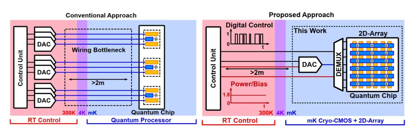
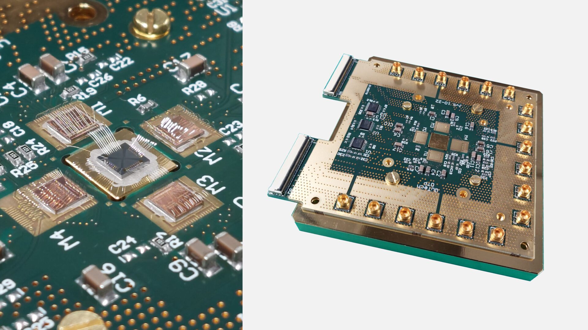
The Cryo-CMOS system, developed in a 22-nm FinFET fabrication process, includes a cryo-CMOS DAC and a demultiplexer. It utilizes a Sample-and-Hold (S/H) circuit, allowing bias voltages to be stored on a hold capacitor and time-multiplexed operations to be used. The system has been successfully demonstrated with a 2D crossbar array of 648 Single Hole Transistors (SHTs) controlled via shared gates. It supports 96 unique bias voltages across a 3V range, with voltage drift between 60 µV/s and 18 mV/s. The system operates at temperatures below 70 mK with total power consumption staying below 120 µW, well within the cooling capacity of the Bluefors LD400 System used in the demonstration.
The team benchmarked the cryo-CMOS system against several leading approaches in cryogenic control electronics, demonstrating a combination of low power, high channel count, and lower operating temperature. Unlike earlier demonstrations that relied on discrete components or room-temperature DACs, this system integrates both the DAC and demultiplexers directly at the millikelvin stage, reducing synchronization complexity and improving signal integrity.
Lead investigator Fabio Sebastiano (TU Delft) explains: ” Cryo-CMOS is emerging as a key enabling technology for large-scale quantum computers and other applications constrained by the wiring bottleneck, such as cryogenic quantum sensors. This work demonstrates that complex functionalities, such as high-resolution high-accuracy voltage generation, can be integrated even at the base temperatures of modern dilution refrigerators. Thanks to its ability to both unlock new possibilities and enhance the reliability, usability, and scalability of existing systems, cryogenic electronics will increasingly become a standard component of cryogenic experiments and infrastructure. “
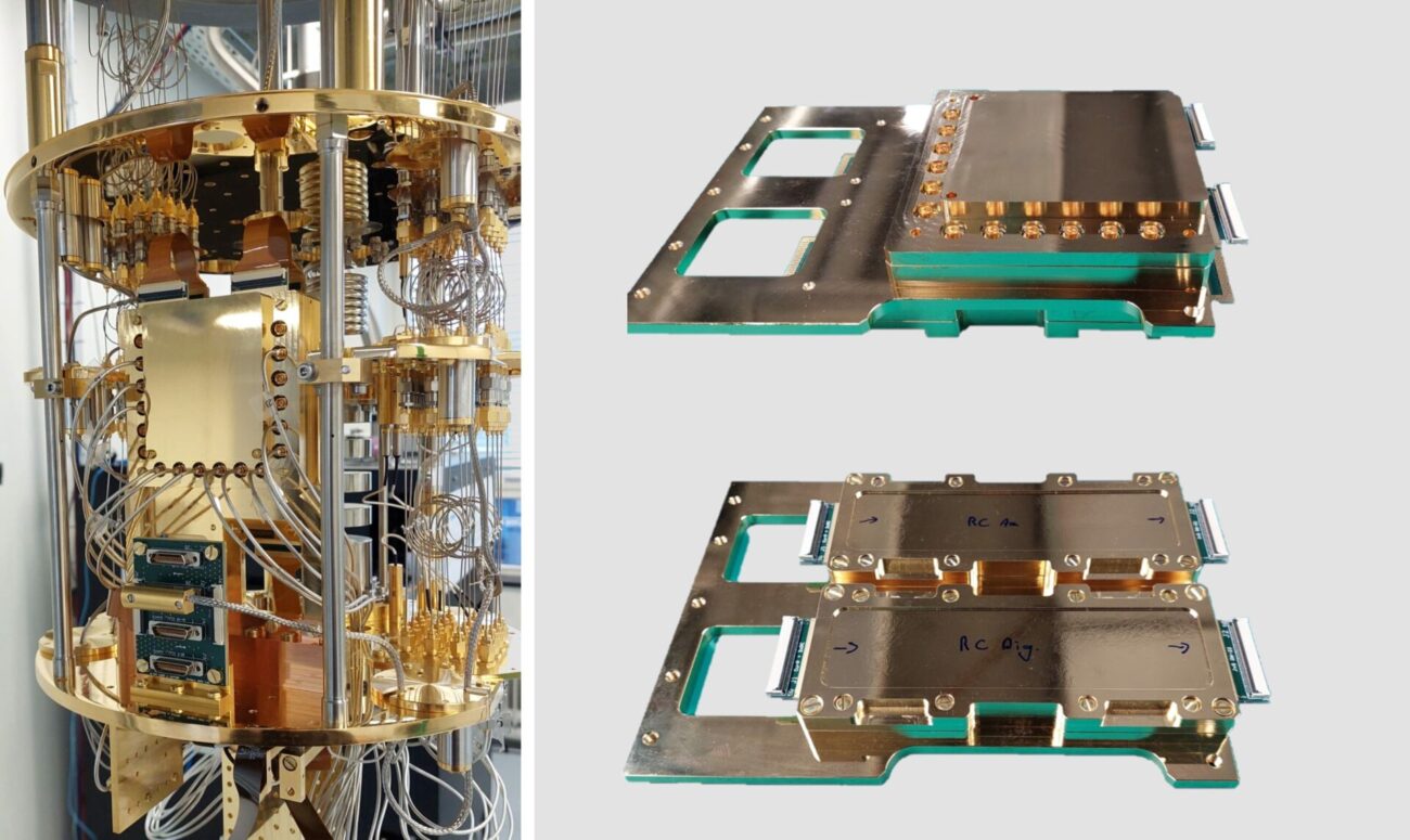
The integration was made possible by a custom-built mechanical and electrical infrastructure mounted directly on the mixing chamber flange of the dilution refrigerator. This setup included a precision-machined copper cold finger for thermal anchoring, a sample PCB with direct chip-to-chip bonding, and dedicated filter boards for signal conditioning. The quantum device chip was attached directly to the copper surface using conductive silver paste to ensure optimal thermal contact, while the cryo-CMOS chips were electrically isolated. Signal routing was carefully separated into shielded analog and digital bundles, with tailored filtering to minimize noise and thermal load. This infrastructure enabled operation of both the quantum devices and the control electronics at 66 mK.
“Alongside the integrated circuit design, we made sure the cryo-CMOS components could be smoothly integrated into the Bluefors system. The Bluefors system is ready for cryo-CMOS—no extra workarounds needed. This technology will be a key enabler for many different quantum computing systems as they scale,” said Russell Lake, Director Quantum Applications at Bluefors.
The work shows that cryo-CMOS electronics can operate directly next to quantum devices, demonstrating a scalable integration of a cryo-CMOS DAC, cryo- CMOS demultiplexer, and crossbar array. By placing control electronics at the same stage as the qubits, the architecture dramatically reduces wiring complexity, addressing a critical bottleneck in scaling semiconductor spin-qubit quantum processors.